Description
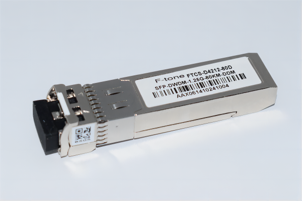
The SFP transceivers are high performance, cost effective modules supporting data-rate of 1250 Mbps and 10km transmission distance on 9/125μm SMF.
The transceiver consists of three sections: a laser transmitter, a PIN photodiode integrated with a trans-impedance preamplifier (TIA) and DDMI control unit. All modules satisfy class I laser safety requirements.
The transceivers are compliant with the Small Form-Factor Pluggable (SFP) Multi-Source Agreement (MSA) and SFF-8472. For further information, please refer to SFP MSA.
Product Features
● Uncooled Laser Diode with MQW Structure
● InGaAs PIN-TIA Photodiode Receiver
● 9/125μm SMF
● Single Mode Transceiver SFP Footprint
● LC Or SC Optical Interface Are Optional
● Compliant With SFP MSA and SFF-8472
● Digital Diagnostic Monitoring Interface
● Single +3.3V Power Supply
● CML Differential Inputs and Outputs
● LVTTL Signal Detection Output
● Compliant With ITU-T G.957
● Compliant With RoHS and Lead Free
● Metal Enclosure for Lower EMI
● Operating Case Temperature:
Standard: 0 to +70°C
Extend: -20 to +85°C
Industrial: -40 to +85°
Product Applications
● Fast Ethernet
● ATM/SONET/SDH
● Switch/Router
● Other Optical Transmission Systems
Absolute Maximum Ratings
|
Parameter |
Symbol |
Min |
Max |
Unit |
|
|
Storage Temperature |
Tst |
-40 |
+85 |
℃ |
|
|
Operating Temperature |
TO |
BYCS-xx12-xxD |
0 |
+70 |
℃ |
|
BYCS-xx12-xxDE |
-20 |
+85 |
℃ |
||
|
BYCS-xx12-xxDI |
-40 |
+85 |
℃ |
||
|
Input Voltage |
- |
GND |
VCC |
V |
|
|
Power Supply Voltage |
VCC-VEE |
0 |
+3.6 |
V |
|
Note: Stress in excess of maximum absolute ratings can cause permanent damage to the module.
Recommended Operating Conditions
|
Parameter |
Symbol |
Min |
Typ |
Max |
Unit |
|
|
Storage Temperature |
Tst |
-40 |
- |
+85 |
℃ |
|
|
Operating Case Temperature |
TC |
BYCS-xx12-xxD |
0 |
- |
+70 |
℃ |
|
BYCS-xx12-xxDE |
-20 |
- |
+85 |
℃ |
||
|
BYCS-xx12-xxDI |
-40 |
- |
+85 |
℃ |
||
|
Power Supply Voltage |
VCC |
3.1 |
3.3 |
3.5 |
V |
|
|
Power Supply Current |
ICC |
- |
- |
300 |
mA |
|
|
Data Rate |
DR |
- |
1250 |
- |
Mbps |
|
Optical Specification
|
Transmitter |
|||||||
|
Parameter |
Symbol |
Min |
Typ |
Max |
Unit |
Note |
|
|
Center Wavelength |
1310 DFB |
lC |
1261 |
1310 |
1360 |
nm |
|
|
Spectral Width |
Dl |
- |
- |
1 |
nm |
- |
|
|
Average Optical Output Power |
Po |
-9.5 |
- |
-3 |
dBm |
||
|
Extinction Ratio |
ER |
9 |
- |
- |
dB |
- |
|
|
Optical Rise/Fall Time(20%-80%) |
Tr/Tf |
- |
- |
0.26 |
ns |
- |
|
|
Output Eye Diagram |
Compliant with ITU-T G.957 |
||||||
|
Receiver |
|||||||
|
Parameter |
Symbol |
Min |
Typ |
Max |
Unit |
Note |
|
|
Operate Wavelength |
- |
1100 |
1310 |
1600 |
nm |
BYCS-1312-xxDx |
|
|
Receiver Sensitivity |
RSENS |
- |
- |
-24 |
dBm |
1 |
|
|
Receiver Saturation |
PRS |
-3 |
- |
- |
dBm |
1 |
|
|
LOS Assert |
- |
-36 |
- |
- |
dBm |
Alarm: High-level |
|
|
LOS De-Assert |
- |
- |
- |
-26 |
dBm |
||
|
LOS Hysteresis |
- |
0.5 |
- |
5 |
dBm |
- |
|
Note: 1. Minimum Sensitivity and saturation levels for a 27-1 PRBS test pattern @1250Mbps.
Electrical Specification
|
Transmitter |
|||||||
|
Parameter |
Symbol |
Min |
Typ |
Max |
Unit |
Note |
|
|
Power Supply Current |
ICCT |
- |
70 |
150 |
mA |
2 |
|
|
Input Differential Impedance |
ZIN |
90 |
100 |
110 |
Ω |
- |
|
|
Input Swing Differential Voltage |
VIN |
500 |
- |
2400 |
mV |
3 |
|
|
TX-Disable Voltage |
Disable |
- |
2.0 |
- |
VCC |
V |
- |
|
Enable |
- |
0 |
- |
0.8 |
V |
- |
|
|
TX-Fault Voltage |
Fault |
- |
2.0 |
- |
VCC |
V |
- |
|
Normal |
- |
0 |
- |
0.8 |
V |
- |
|
|
Receiver |
|||||||
|
Parameter |
Symbol |
Min |
Typ |
Max |
Unit |
Note |
|
|
Power Supply Current |
ICCR |
- |
70 |
140 |
mA |
2 |
|
|
Output Swing Differential Voltage |
VOUT |
600 |
- |
2000 |
mV |
4 |
|
|
LOS Voltage |
High |
- |
2.0 |
- |
VCC |
V |
- |
|
Low |
- |
0 |
- |
0.8 |
V |
- |
|
Note:
2. The current excludes the output load current.
3. CML input, internally AC-coupled and terminated.
4. Internally AC-coupled.
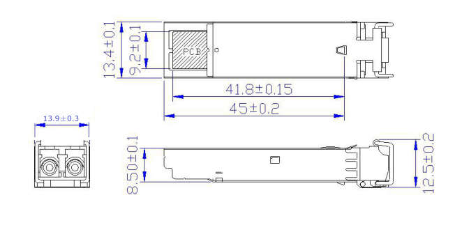
Package Diagram
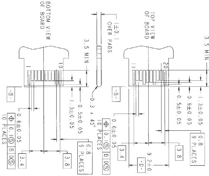
Board Layout Hole Pattern
LC Side Interface
Order Information
|
产品型号 |
封装 |
波长(-xx) |
速率(xx) |
传输距离 (-xx) |
x |
等级(x) |
|
BYCS-1312-20Dxx |
SFP |
13=1310nm |
12=1250Mbps |
20=20km |
空 不带DDM |
空 商业级 |


