Features
● 10Gb/s serial optical interface compliant to 802.3ae 10GBASE-SR
● Electrical interface compliant to SFF-8431 specifications for enhanced 8.5 and 10 Gigabit small form factor pluggable module “SFP+”
● 850nm VCSEL transmitter, PIN photo-detector
● 2-wire interface for management specifications compliant with SFF 8472 digital diagnostic monitoring interface for optical transceivers
● Operating case temperature: -5 to 75 °C
● All-metal housing for superior EMI performance
● Low power consumption
● Advanced firmware allow customer system encryption information to be stored in transceiver
● Cost effective SFP+ solution, enables higher port densities and greater bandwidth
● RoHS compliant
Applications
● High-speed storage area networks
● Computer cluster cross-connect
● Custom high-speed data pipes
● 10GE Storage, 8G Fiber Channel
● Inter Rack Connection
ABSOLUTE MAXIMUM RATING
These values represent the damage threshold of the module. Stress in excess of any of the individual Absolute Maximum Ratings can cause immediate catastrophic damage to the module even if all other parameters are within Recommended Operating Conditions.
|
Parameters |
Symbol |
Min. |
Max. |
Unit |
|
Power Supply Voltage |
VCC |
0 |
3.6 |
V |
|
Storage Temperature |
Tc |
-40 |
85 |
。C |
|
Operating Case Temperature |
Tc |
-5 |
75 |
。C |
|
Relative Humidity |
RH |
5 |
95 |
% |
|
RX Input Average Power |
Pmax |
- |
0 |
dBm |
RECOMMENDED OPERATING ENVIRONMENT
Recommended Operating Environment specifies parameters for which the electrical and optical characteristics hold unless otherwise noted.
|
Parameters |
Symbol |
Min. |
Typical |
Max |
Unit |
|
Power Supply Voltage |
VCC |
3.135 |
3.3 |
3.465 |
V |
|
Operating Case Temperature |
TC |
-5 |
25 |
75 |
。C |
OPTICAL CHARACTERISTICS
The following optical characteristics are defined over the Recommended Operating Environment unless otherwise specified.
|
Parameter |
Symbol |
Min. |
Typical |
Max |
Unit |
Notes |
|
Transmitter |
||||||
|
Center Wavelength |
λt |
840 |
850 |
860 |
nm |
|
|
RMS spectral width |
Pm |
- |
- |
Note 1 |
nm |
|
|
Average Optical Power |
Pavg |
-6.5 |
- |
-1 |
dBm |
|
|
Optical Power OMA |
Poma |
- |
- |
Note 1 |
dBm |
|
|
Extinction Ratio |
ER |
3.5 |
- |
- |
dB |
|
|
Transmitter Dispersion Penalty |
TDP |
- |
- |
3.9 |
dB |
|
|
Relative Intensity Noise |
Rin |
- |
- |
-128 |
dB/Hz |
12dB reflection |
|
Optical Return Loss Tolerance |
- |
- |
12 |
dB |
||
|
Receiver |
||||||
|
Center Wavelength |
λr |
840 |
850 |
860 |
nm |
|
|
Receiver Sensitivity(OMA) |
Psens |
- |
- |
-11.1 |
dBm |
|
|
Stressed Sensitivity(OMA) |
- |
- |
-7.5 |
dBm |
||
|
Los function |
Los |
-30 |
- |
-12 |
dBm |
|
|
Overload |
Pin |
- |
- |
-1 |
dBm |
|
|
Receiver Reflectance |
- |
- |
-12 |
dB |
||
* Note 1: Trade-offs are available between spectral width, center wavelength and minimum OMA, as shown in table 6.
Table 6: Minimum 10GBASE-SR OMA as a Function of Wavelength and Spectral Widt
|
Center Wavelength(nm) |
RMS Spectral width (nm) |
||||||||
|
Up to 0.05 |
0.05 to 0.1 |
0.1 to 0.15 |
0.15 to 0.2 |
0.2 to 0.25 |
0.25 to 0.3 |
0.3 to 0.35 |
0.35 to 0.4 |
0.4 to 0.45 |
|
|
840 to 842 |
-4.2 |
-4.2 |
-4.1 |
-4.1 |
-3.9 |
-3.8 |
-3.5 |
-3.2 |
-2.8 |
|
842 to 844 |
-4.2 |
-4.2 |
-4.2 |
-4.1 |
-3.9 |
-3.8 |
-3.6 |
-3.3 |
-2.9 |
|
844 to 846 |
-4.2 |
-4.2 |
-4.2 |
-4.1 |
-4 |
-3.8 |
-3.6 |
-3.3 |
-2.9 |
|
846 to 848 |
-4.3 |
-4.2 |
-4.2 |
-4.1 |
-4 |
-3.8 |
-3.6 |
-3.3 |
-2.9 |
|
848 to 850 |
-4.3 |
-4.2 |
-4.2 |
-4.1 |
-4 |
-3.8 |
-3.6 |
-3.3 |
-3 |
|
850 to 852 |
-4.3 |
-4.2 |
-4.2 |
-4.1 |
-4 |
-3.8 |
-3.6 |
-3.4 |
-3 |
|
852 to 854 |
-4.3 |
-4.2 |
-4.2 |
-4.1 |
-4 |
-3.9 |
-3.7 |
-3.4 |
-3.1 |
|
854 to 856 |
-4.3 |
-4.3 |
-4.2 |
-4.1 |
-4 |
-3.9 |
-3.7 |
-3.4 |
-3.1 |
|
856 to 858 |
-4.3 |
-4.3 |
-4.2 |
-4.1 |
-4 |
-3.9 |
-3.7 |
-3.5 |
-3.1 |
|
858 to 860 |
-4.3 |
-4.3 |
-4.2 |
-4.2 |
-4.1 |
-3.9 |
-3.7 |
-3.5 |
-3.2 |
ELECTRICAL CHARACTERISTICS
The following electrical characteristics are defined over the Recommended Operating Environment unless otherwise specified.
|
Parameter |
Symbol |
Min. |
Typical |
Max |
Unit |
Notes |
|
Data Rate |
- |
10.3125 |
- |
Gbps |
||
|
Power Consumption |
- |
600 |
800 |
mW |
||
|
Transmitter |
||||||
|
Single Ended Output Voltage Tolerance |
-0.3 |
- |
4 |
V |
||
|
C common mode voltage tolerance |
15 |
- |
- |
mV |
||
|
Tx Input Diff Voltage |
VI |
180 |
800 |
mV |
||
|
Tx Fault |
VoL |
-0.3 |
0.4 |
V |
At 0.7mA |
|
|
Data Dependent Input Jitter |
DDJ |
0.1 |
UI |
|||
|
Data Input Total Jitter |
TJ |
0.28 |
UI |
|||
|
Receiver |
||||||
|
Single Ended Output Voltage Tolerance |
-0.3 |
- |
4 |
V |
||
|
Rx Output Diff Voltage |
Vo |
300 |
850 |
mV |
||
|
Rx Output Rise and Fall Time |
Tr/Tf |
30 |
ps |
20% to 80% |
||
|
Total Jitter |
TJ |
0.7 |
UI |
|||
|
Deterministic Jitter |
DJ |
0.42 |
UI |
|||
MECHANICAL
Comply to SFF-8432 rev. 5.0, the improved Pluggable form factor specification.
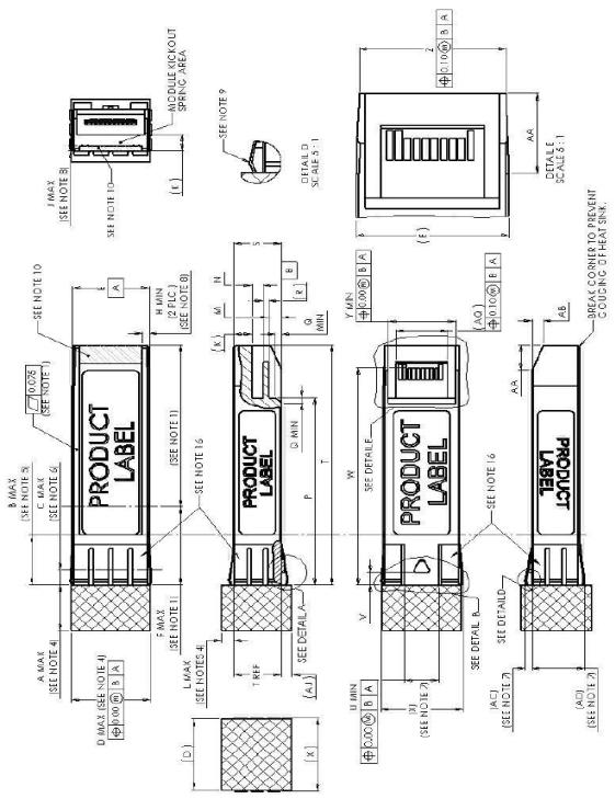
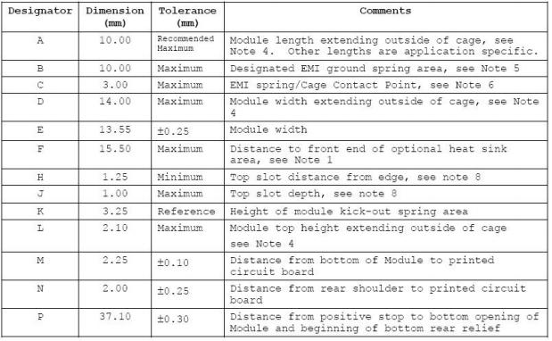 Key Mechanical Dimensions
订单信息
|
产品型号 |
封装 |
波长(-xx) |
速率(xx) |
传输距离 (-xx) |
x |
等级(x) |
|
BYCS-M131X-02Dxx |
SFP+ |
85=850nm |
1X=10.3GBP/s |
02=300m |
空 不带DDM |
空 商业级 |