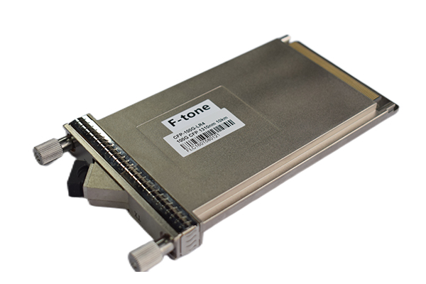
Description
The F-tone Networks 100GBASE-LR4 CFP module is the CFP optical transceiver which is a hot pluggable form factor designed for high speed optical networking application. The module is designed for 100Gigabit Ethernet application and provides 100GBASE-LR4 compliant optical interface, CAUI electrical interface and MDIO module managementinterface. The module converts 10-lane 10.3Gb/s electrical data streams to 4-lane LAN-WDM25.78Gb/s optical output signal and4-laneLAN-WDM25.78Gb/s optical inputsignal to 10-lane10.3Gb/s electrical data streams. This 10-lane 10.3Gb/s electrical signal is fully compliant with802.3ba CAUI specification and allows FR4 host PCB trace up to 25cm. The high performance Cooled LAN-WDM EML transmitter and high sensitivity PIN receiver provide superior performance for 100Gigabit Ethernet applications up to 10km links and compliant optical interface with IEEE802.3ba Clause 88 100GBASE-LR4 requirements.
Features
● Operating optical data rate up to 112Gbps
● Transmission distance up to 10km
● CFP MSA compliant
● Compliant to 100GbE IEEE 802.3ba specification for 100GBASE-LR4 links
● OTU4 compatible
● 1310 nm window cooled EA-DFB LD and PIN ROSA
● 10 parallel electrical serial interface and AC coupling of CML signals
● Hot pluggable electrical interface
● Low power dissipation<9W
● Single 3.3V power supply
● RoHS 6 compliant(lead free)
● Case operating temperature
Commercial: 0 ~ +70℃
Industrial: -40 ~ +85℃
Applications
● 100GbE IEEE 802.3ba 100GBASE-LR4
● OTN-OTU4
● Switch to switch interface or Switch to router interface
Absolute Maximum Ratings
|
Parameter |
Symbol |
Unit |
Min |
Max |
|
Storage Temperature Range |
Ts |
°C |
-40 |
+85 |
|
Relative Humidity |
RH |
% |
5 |
85 |
|
Power Supply Voltage |
Vcc |
V |
-0.5 |
+ 3.6 |
|
Operating Case Temperature Range |
Tc |
°C |
-5 |
75 |
|
Receiver Damage Threshold Per Lane |
Pdag |
dBm |
+5.5 |
Recommended Operating Conditions
|
Parameter |
Symbol |
Unit |
Min |
Typ |
Max |
|
Operating Case Temperature Range |
Tc |
oC |
0 |
70 |
|
|
Power Supply Voltage |
Vcc |
V |
3.2 |
3.3 |
3.4 |
|
Data rate |
Gb/s |
103.125 |
112 |
Products Characteristics(tested under recommended operating conditions)
|
Parameter |
Symbol |
Unit |
Min |
Typ |
Max |
Notes |
|
Voltage Supply Electrical Characteristics |
||||||
|
Supply Current Tx Section / Rx Section |
a |
- |
- |
3 |
1 |
|
|
Power Supply Noise |
Vrip |
2% |
DC-1MHz |
|||
|
3% |
1-10MHz |
|||||
|
Dissipation Class2 |
Pw |
W |
9 |
|||
|
Low Power Dissipation |
Plow |
W |
2 |
|||
|
Inrush Current n 2 |
I-inrush mA/usec |
50 |
||||
|
Turn-off Current Class2 |
I-turnoff mA/usec |
-50 |
||||
|
Different Signal Electrical Characteristics |
||||||
|
Single Ended Data Input Swing |
mV |
55 - |
525 |
|||
|
Single Ended Data Output Swing |
mV |
180 - |
385 |
|||
|
Differential Signal Resistance |
Output |
Ω |
80 |
120 |
||
|
Differential Signal Resistance |
Input |
Ω |
80 |
120 |
||
|
3.3V LVCMOS Electrical Characteristics |
||||||
|
Input High Voltage |
3.3VIH |
V |
2.0 |
Vcc+0.3 |
||
|
Input Low Voltage |
3.3VIL |
V |
-0.3 - |
0.8 |
||
|
Input Leakage Current |
3.3IIN |
uA |
-10 |
+ 10 |
||
|
Output HighVoltage(Ioh=100uA) |
3.3VOH |
V |
Vcc-0.2 - |
- |
||
|
Output Low Voltage (Ioi = 100uA) |
3.3VOL |
V |
0.2 |
|||
|
Minimum Pulse Width of Control Pin Signal |
T_CNTL |
us |
100 |
|||
|
1.2V LVCMOS Electrical Characteristics |
||||||
|
Input High Voltage |
1.2VIH |
V |
0.84 |
1.5 |
||
|
Input Low Voltage |
1.2VIL |
V |
-0.3 |
0.36 |
||
|
Input Leakage Current |
1.2IIN |
uA |
-100 |
+ 100 |
||
|
Output HiqhVoltaqe |
1.2VOH |
V |
1.0 |
1.5 |
||
|
Output Low Voltaqe |
1.2VOL |
V |
-0.3 |
0.2 |
||
|
Output Hiqh Current |
1.2IOH |
mA |
-4 |
|||
|
Output Low Current |
1.2IOL |
mA |
+4 |
|||
|
Input Capacitance |
Ci |
pF |
10 |
|||
|
Optical Transmitter Characteristics |
||||||
|
Signaling Rate for Each Lane (100GbE) |
Gbps |
- |
25.78125+/-100ppm |
|||
|
Signaling Rate for Each Lane (OTU4) |
27.95249+/-20ppm |
|||||
|
Four Lane Wavelength Range |
入1 |
nm |
1294.53 |
1295.56 |
1296.59 |
|
|
入2 |
1299.02 |
1300.05 |
1301.09 |
|||
|
入3 |
1303.54 |
1304.58 |
1305.63 |
|||
|
入4 |
1308.09 |
1309.14 |
1310.19 |
|||
|
Side Mode Suppression Ratio |
SMSR |
dB |
30 |
- |
||
|
Total Average Launch Power(100GbE) |
Pt |
dBm |
- |
10.5 |
||
|
Total Average Launch Power(OTU4) |
8.9 |
|||||
|
Average Launch Power for Each Lane(100GbE) |
Pa |
dBm |
-4.3 |
+4. 5 |
2 |
|
|
Average Launch Power for Each Lane(OTU4) |
-2.5 |
+2.9 |
||||
|
Optical Modulation Amplitude for Each Lane |
OMA |
dBm |
-1.3 |
4.5 |
3 |
|
|
Transmitter and Dispersion Penalty for Each Lanes(100GbE) |
TDP |
2.2 |
||||
|
Transmitter and Dispersion Penalty for Each Lanes(OTU4) |
TDP |
1.5 |
||||
|
Average Launch Power of Off Transmitter for Each Lanes |
Poff |
dBm |
- |
-30 |
||
|
Extinction Ratio (100GbE) |
EX |
dB |
4 |
|||
|
Extinction Ratio (OTU4) |
7 |
|||||
|
Maximum channel power difference |
dB |
5 |
||||
|
RIN20OMA |
dB/Hz |
-130 |
||||
|
Optical Return Loss Tolerance |
dB |
20 |
||||
|
Transmitter Reflectance |
dB |
-12 |
4 |
|||
|
Eye Diagram |
Compliant with IEEE 802.3ba-2010/G.959.1) |
|||||
|
Optical Receiver Characteristics |
||||||
|
Receive Rate for Each Lane(100GbE) |
Gbps |
25.78125+/-100ppm |
||||
|
Receive Rate for EachLane(OTU4) |
27.95249+/-20ppm |
|||||
|
Four Lane Wavelength Range |
入1 |
1294.53 |
1295.56 |
1296.59 |
||
|
入2 |
nm |
1299.02 |
1300.05 |
1301.09 |
||
|
入3 |
1303.54 |
1304.58 |
1305.63 |
|||
|
入4 |
1308.09 |
1309.14 |
1310.19 |
|||
|
Overload Input Optical Power |
Pmax |
dBm |
4.5 |
5 |
||
|
Total Input Optical Power(OTU4) |
Pt |
dBm |
8.9 |
|||
|
Average Receive Power for Each Lane(100GbE) |
Pin |
dBm |
-10.6 |
4.5 |
6&7 |
|
|
Average Receive Power for Each Lane(OTU4) |
-8.8 |
2.9 |
||||
|
Receive Power In OMA for Each Lane |
PinOMA |
dBm |
- |
4.5 |
||
|
Difference in Receive Power between Any Two Lanes |
dBm |
- |
5.5 |
|||
|
Receiver Sensitivity in OMA for Each lanellanelabLane(100GbE) |
Pmin |
dBm |
-8.6 |
8 |
||
|
Receiver Sensitivity for Each Lane(OTU4) |
-10.3 |
9 |
||||
|
StressedReceiver Sensitivity in OMA for Each Lane |
dBm |
-6.8 |
10&11 |
|||
|
Los Assert |
dBm |
-20 |
-15 |
|||
|
Los De-assert |
dBm |
-14 |
||||
|
Los Hysteresis |
dBm |
0.5 |
||||
|
Chromatic Dispersion |
Ps/nm |
-28.5 |
+9.5 |
|||
|
Maximum reflectance of optical network element |
dB |
-26 |
||||
|
Delay Group differencial |
ps |
8 |
||||
Note1. The supply current includes CFP module's supply current and test board working current.
Note2. Average launch power ,each lane(min) is informative and not the principal indicator of signal strength. A transmitter with launch power below this value cannot be compliant;however, a value above this does not ensure compliance
Note3. Even if the TDP<1dB, the OMA(min) must exceed this value
Note4. Transmitter reflectance is defined looking into the transmitter
Note5. The receiver shall be able to tolerate , without damage, continuous exposure to an optical input signal having this average power level
Note6. The average receive power , each lane (max) for 100GBASE-ER4 is larger than the 100BASE-ER4 transmitter value to allow compatibility with 100BASE-LR4 units at short distances
Note7. Average receive power, each lane (min) is informative and not the principal indicator of signal strength. A received power below this value cannot be compliant; however, a value above this does not ensure compliance
Note8. Receiver sensitivity (OMA), each lane (max) is informative
Note9. Measured with PRBS 231-1 for BER=10-5. The BER for the OTU4 application is required to be met only after FEC has been applied.
Note10. Measured with conformance test signal at TP3 for BER=10-12 Note11. conditions of stressed receiver sensitivity test: vertical eye closure penalty for each lane is 1.8dB;stressed eye J2 jitter for each lane is 0.3UI; stressed eye J9 jitter for each lane is 0.47UI.
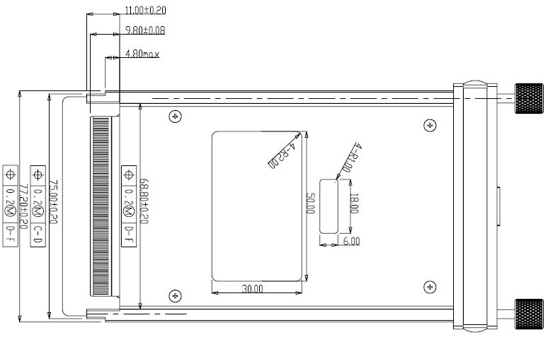
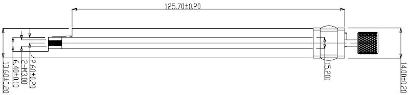
Mechanical Dimensions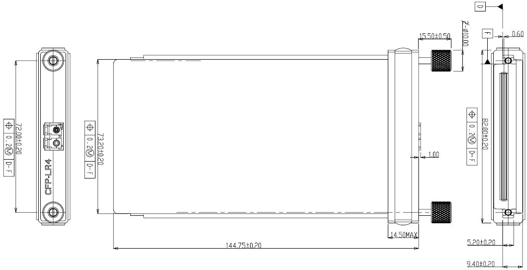
Ordering information
|
Part Number |
Product Description |
|
FTC1-HG-LR4 |
CFP, 100GE/OTU4,10km,100GBASE-LR4, Pout -4.3 ~ +4.5 PIN <-8.6dBm,0ºC ~ +70ºC |
|
FTC1-HG-LR4I |
CFP, 100GE/OTU4,10km,100GBASE-LR4, Pout -4.3 ~ +4.5 PIN <-8.6dBm,-40ºC ~ +85ºC |
北亿纤通 | F-tone Networks
企业邮箱: 该邮件地址已受到反垃圾邮件插件保护。要显示它需要在浏览器中启用 JavaScript。
企业手机:19081343401
企业电话:028-85255257
企业传真:028-85977702
注:本产品有全国产化型号可选
本产品为CFP光模块,仅展示部分参数,如有需要,请联系我们。
Important Notice
Performance figures, data and any illustrative material provided in this data sheet are typical and must be specifically confirmed in writing by F-tone Networks before they become applicable to any particular order or contract. In accordance with the F-tone Networks policy of continuous improvement specifications may change without notice.
The publication of information in this data sheet does not imply freedom from patent or other protective rights of F-tone Networks or others. Further details are available from any F-tone Networks sales representative.